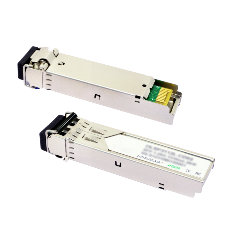
Mylinking™ Optical Transceiver Module SFP LC-MM 850nm 550m
ML-SFP-MX 1.25Gbps SFP 850nm 550m LC Multi-Mode
Product Features
● Supports 1.25Gbps/1.0625Gbps bit rates
● Duplex LC connector
● Hot pluggable SFP footprint
● 850nm VSCEL laser transmitter and PIN photo-detector
● Applicable for 550m on 50/125µm, 300m on 62.5/125µm MMF connection
● Low power consumption, < 0.8W
● Digital Diagnostic Monitor Interface
● Compliant with SFP MSA and SFF-8472
● Very low EMI and excellent ESD protection
● Operating case temperature:
Commerical:0 to 70 °C
Industrial:-40 to 85 °C
Applications
● Gigabit Ethernet
● Fiber Channel
● Switch to Switch interface
● Switched backplane applications
● Router/Server interface
● Other optical transmission systems
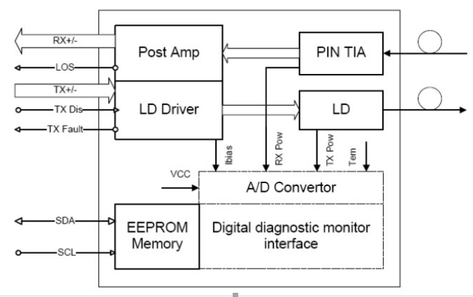
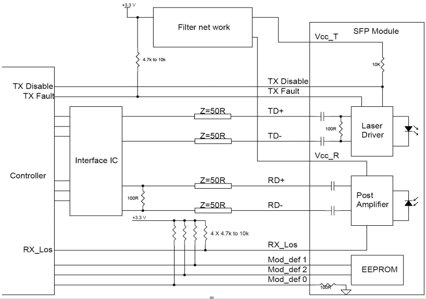
Functional Diagram
Absolute Maximum Ratings
|
Parameter |
Symbol |
Min. |
Max. |
Unit |
Note |
| Supply Voltage |
Vcc |
-0.5 |
4.0 |
V |
|
| Storage Temperature |
TS |
-40 |
85 |
°C |
|
| Relative Humidity |
RH |
0 |
85 |
% |
Note: Stress in excess of the maximum absolute ratings can cause permanent damage to the transceiver.
General Operating Characteristics
|
Parameter |
Symbol |
Min. |
Typ |
Max. |
Unit |
Note |
| Data Rate |
DR |
|
1.25 |
|
Gb/s |
|
| Supply Voltage |
Vcc |
3.13 |
3.3 |
3.47 |
V |
|
| Supply Current |
Icc5 |
|
220 |
mA |
||
| Operating Case Temp. |
Tc |
0 |
70 |
°C |
||
|
TI |
-40 |
85 |
Electrical Characteristics (TOP(C) = 0 to 70 ℃, TOP(I) =-40 to 85 ℃,VCC = 3.13 to 3.47 V)/h2>
|
Parameter |
Symbol |
Min. |
Typ |
Max. |
Unit |
Note |
|
|
Transmitter |
|||||||
| Differential data input swing |
VIN,PP |
250 |
|
1200 |
mVpp |
1 |
|
| Tx Disable Input-High |
VIH |
2.0 |
|
Vcc+0.3 |
V |
||
| Tx Disable Input-Low |
VIL |
0 |
|
0.8 |
V |
||
| Tx Fault Output-High |
VOH |
2.0 |
|
Vcc+0.3 |
V |
2 |
|
| Tx Fault Output-Low |
VOL |
0 |
|
0.8 |
V |
2 |
|
| Input differential impedance |
Rin |
|
100 |
|
Ω |
||
|
Receiver |
|||||||
| Differential data output swing |
Vout,pp |
250 |
|
550 |
mVpp |
3 |
|
| Rx LOS Output-High |
VROH |
2.0 |
|
Vcc+0.3 |
V |
2 |
|
| Rx LOS Output-Low |
VROL |
0 |
|
0.8 |
V |
2 |
|
Notes:
1. TD+/- are internally AC coupled with 100Ω differential termination inside the module.
2. Tx Fault and Rx LOS are open collector outputs, which should be pulled up with 4.7k to 10kΩ resistors on the host board. Pull up voltage between 2.0V and Vcc+0.3V.
3.RD+/- outputs are internally AC coupled, and should be terminated with 100Ω (differential) at the user SERDES.
Optical Characteristics (TOP(C) = 0 to 70 ℃, TOP(I) =-40 to 85 ℃,VCC = 3.13 to 3.47 V)
|
Parameter |
Symbol |
Min. |
Typ |
Max. |
Unit |
Note |
|
Transmitter |
||||||
| Operating Wavelength |
λ |
840 |
850 |
860 |
nm |
|
| Ave. output power (Enabled) |
PAVE |
-9 |
0 |
dBm |
1 |
|
| Extinction Ratio |
ER |
9 |
|
|
dB |
1 |
| RMS spectral width |
Δλ |
0.65 |
nm |
|||
| Rise/Fall time (20%~80%) |
Tr/Tf |
0.25 |
ps |
2 |
||
| Output Optical Eye | Compliant with IEEE802.3 z &ITU G.957 Compliant (class 1 aser safety) | |||||
|
Receiver |
||||||
| Operating Wavelength |
λ |
840 |
850 |
860 |
nm |
|
| Receiver Sensitivity |
PSEN1 |
-18 |
dBm |
3 |
||
| Overload |
PAVE |
-3 |
|
dBm |
3 |
|
| LOS Assert |
Pa |
-35 |
dBm |
|||
| LOS De-assert |
Pd |
-20 |
dBm |
|||
| LOS Hysteresis |
Pd-Pa |
0.5 |
|
dB |
||
Notes:
1. Measured at 1.25Gb/s with PRBS 223 – 1 NRZ test pattern.
2.Unfiltered, measured with a PRBS 223-1 test pattern @1.25Gbps
3.Measured at 1.25Gb/s with PRBS 223 – 1 NRZ test pattern for BER < 1x10⁻¹⁰
Pin Definitions And Functions
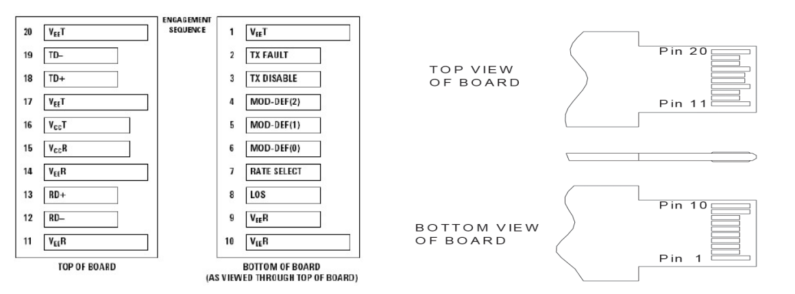
|
Pin |
Symbol |
Name/Description |
Notes |
| 1 | VeeT | Tx ground |
|
| 2 | Tx Fault | Tx fault indication, Open Collector Output, active “H” |
1 |
| 3 | Tx Disable | LVTTL Input, internal pull-up, Tx disabled on “H” |
2 |
| 4 | MOD-DEF2 | 2 wire serial interface data input/output (SDA) |
3 |
| 5 | MOD-DEF1 | 2 wire serial interface clock input (SCL) |
3 |
| 6 | MOD-DEF0 | Model present indication |
3 |
| 7 | Rate select | No connection |
|
| 8 | LOS | Rx loss of signal, Open Collector Output, active “H” |
4 |
| 9 | VeeR | Rx ground |
|
| 10 | VeeR | Rx ground |
|
| 11 | VeeR | Rx ground |
|
| 12 | RD- | Inverse received data out |
5 |
| 13 | RD+ | Received data out |
5 |
| 14 | VeeR | Rx ground |
|
| 15 | VccR | Rx power supply |
|
| 16 | VccT | Tx power supply |
|
| 17 | VeeT | Tx ground |
|
| 18 | TD+ | Transmit data in |
6 |
| 19 | TD- | Inverse transmit data in |
6 |
| 20 | VeeT | Tx ground |
Notes:
1. When high, this output indicates a laser fault of some kind. Low indicates normal operation. And should be pulled up with a 4.7 – 10KΩ resistor on the host board.
2. TX disable is an input that is used to shut down the transmitter optical output. It is pulled up within the module with a 4.7 – 10KΩ resistor. Its states are:
Low (0 – 0.8V): Transmitter on (>0.8, < 2.0V): Undefined
High (2.0V~Vcc+0.3V): Transmitter Disabled Open: Transmitter Disabled
3. Mod-Def 0,1,2. These are the module definition pins. They should be pulled up with a 4.7K – 10KΩ resistor on the host board. The pull-up voltage shall be between 2.0V~Vcc+0.3V.
Mod-Def 0 has been grounded by the module to indicate that the module is present
Mod-Def 1 is the clock line of two wire serial interface for serial ID
Mod-Def 2 is the data line of two wire serial interface for serial ID
4. When high, this output indicates loss of signal (LOS). Low indicates normal operation.
5. RD+/-: These are the differential receiver outputs. They are AC coupled 100Ω differential lines which should be terminated with 100Ω (differential) at the user SERDES. The AC coupling is done inside the module and is thus not required on the host board.
6. TD+/-: These are the differential transmitter inputs. They are AC-coupled, differential lines with 100Ω differential termination inside the module. The AC coupling is done inside the module and is thus not required on the host board.
Typical Interface Circuit
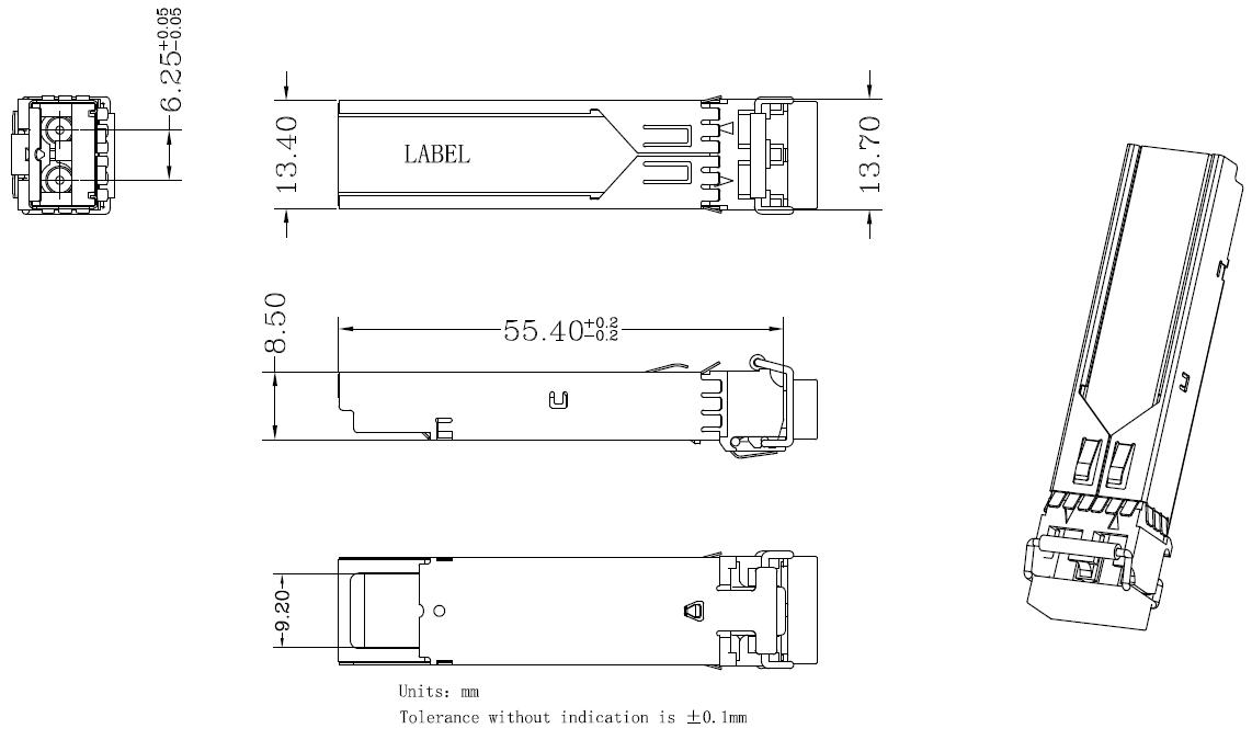
Package Dimensions